Beam-Exit Cross-Sectional Polishing
BEXP
Beam-exit cross-sectional polishing is a patented oblique cutting and polishing technique that provides near-atomically-flat cross-sections of multilayer materials and devices. Cross-sections start from a few nm below the surface and can extend to depths of several microns. The cross-sectional surface is well suited for study with optical microscopy, scanning electron microscopy (SEM) and scanning probe microscopy (SPM) by either the customer or LMA's skilled team.
Background
The conventional approach to imaging and fault analysis of multilayer structures and device is focused ion-beam (FIB) sectioning followed by scanning electron microscopy (SEM) ot transmission electron microscopy (TEM). Ga-ion FIB typically produces a narrow cut (~10um wide), and implants Ga atoms in the cut, affecting the mechanical, thermal and electrical properties. Ar-ion sectioning is gentler, but the conventional perpendicular-to-the-surface geometry damages the first few microns close to the surface and is therefoe only suitable for bulk materials, packaging, solder joints, etc.
Our Solution
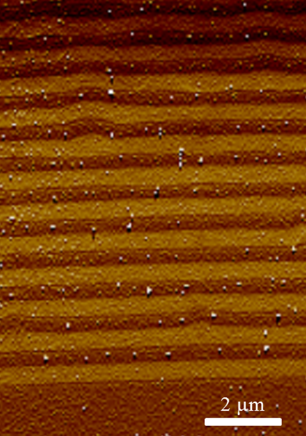
Our patented Ar-ion BEXP technique creates an oblique cross-sectional surface with sub-nm roughness. Sample damage is minimal due to the grazing angle of the beam and the inert nature of Ar. The cross-section runs from the immediate sample surface to ~25 um in depth, and extends 500-1000 um in width, creating a large area for the detailed study of the sample. The shallow angle of the cross-section allows easy SEM and SPM investigation of layers only a few nm in thickness. The grazing incidence of the Ar-ion beam also stretches out the features (e.g. a 2-nm-thick layer creates a ~10-12 nm band in the oblique section), but still allows the sub-nm precision of the vertical (z) movement of the SPM probe to be used, for example to measure layer thicknesses. This means that BEXP + SPM can be accurate as TEM for determining thickness of layers nm-scale layers, but with faster turnaround, lower cost and, significantly, about 1000x wider analysis area.


Nanoscale Characterisation
BEXP preserves material properties, while the shallow-angle geometry allows the use of a range of high-sensitivity nanoscale SPM mapping techniques to determine physical as well as morphological properties of buried layers or features, including:
• Structural: morphology and layer thickness via materials sensitive contrast.
• Nanomechanical: sensitivity to near-surface changes in elastic moduli of materials, near-surface voids and delaminations.
• Nanothermal: sensitivity to thermal conductivity of materials.
• Nanoelectrical: sensitivity to local potential and electrical conductivity
Materials or Devices
LMA’s exclusive BEXP technique combined with its world-leading expertise in structural, thermal, mechanical and electrical SPM characterisation has already been successfully applied to a range of materials and devices:
• MBE and MOCVD grown structures such as LEDs, multi-junction solar cells and vertical-cavity surface-emitting lasers;
• High-aspect ratio porous silicon structures;
• Heat-assisted magnetic recording media;
• Thermal interface materials;
• Glass coatings;
• Phase change memories.